Global Atomic Layer Deposition (ALD) Equipment Market
Global Atomic Layer Deposition Equipment Market Size, Share By Equipment Type (Single-wafer ALD Systems, Batch ALD Systems, Spatial ALD Systems, Roll-to-roll ALD Systems), By Technology Type (Thermal ALD, Plasma-enhanced ALD (PEALD)), By Wafer Size (300 mm, 200 mm, Below 200 mm), and By Region (North America, Europe, Asia-Pacific, Latin America, Middle East & Africa), Analysis and Forecast 2026-2035.
CAGR
10.93%
REVENUE 2025
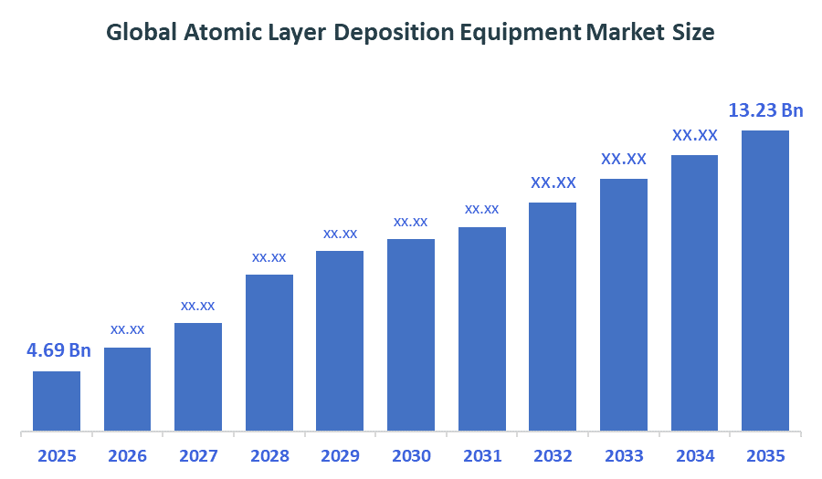
USD Billion 4.69
FORECAST 2035
USD Billion 13.23
REPORT COVERAGE
Global
Market Snapshot
- Global Atomic Layer Deposition Equipment Market Size (2025): USD 4.69 Billion
- Projected Global Atomic Layer Deposition Equipment Market Size (2035): USD 13.23 Billion
- Global Atomic Layer Deposition Equipment Market Compound Annual Growth Rate (CAGR): 10.93%
- Largest Regional Market: Asia Pacific
- 2nd Largest Region: North America
- Fastest Growing Region: Europe
- Base Year: 2025
- Historical Period: 2021-2024
- Market Forecast Period: 2026-2035
Market Overview/ Introduction
The Global Atomic Layer Deposition (ALD) Equipment Market includes thin-film deposition systems that produce atomic-level uniform ultra-thin coatings needed for semiconductor, electronic and energy storage and advanced materials applications. The market experiences strong growth because customers need smaller electronic parts and better chip production methods, and future semiconductor technologies. Government initiatives such as the U.S. CHIPS and Science Act, EU semiconductor programs, and Asia-Pacific manufacturing incentives are accelerating domestic chip production and boosting ALD equipment adoption. Leading companies are investing in advanced plasma-enhanced ALD systems, automation, and AI-driven process control to improve efficiency and scalability. The market provides benefits through its exceptional film distribution, precise measurement capabilities and its ability to handle complicated device designs. The market will grow because of rising semiconductor requirements and new manufacturing facilities, and expanding uses in energy storage, healthcare devices and nanotechnology innovations throughout the world.
- Applied Materials invested USD 4 billion in Montana expansion, while ASM acquired Forge Nano to advance spatial ALD, enhancing semiconductor manufacturing capacity and deposition technology innovation globally.
- Asia-Pacific initiatives include strong government investments in Taiwan, South Korea, and China to expand semiconductor production capacity, increasing demand for advanced manufacturing tools and accelerating growth of ALD equipment adoption.
Notable Insights: -
- Asia Pacific is anticipated to hold approximately 38% share of the global atomic layer deposition equipment market over the predicted timeframe.
- North America is expected to grow at a rapid CAGR in the global atomic layer deposition equipment market by holding approximately 30% of the share during the forecast period.
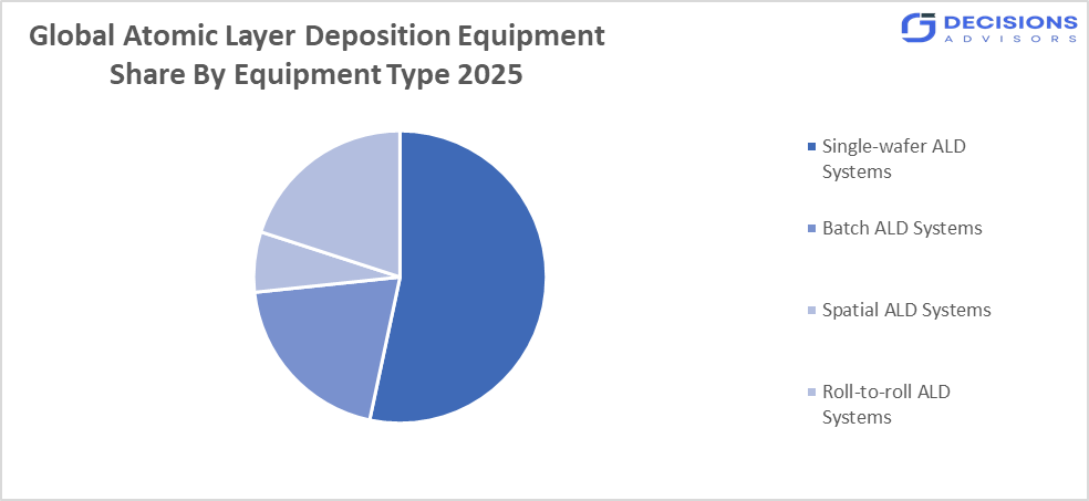
- By equipment type, the single-wafer ALD systems segment dominated the market and holds approximately 48% share in 2025 and is projected to grow at a substantial CAGR during the forecast period.
- By technology type, the PEALD segment dominated the market and holds approximately 55% share in 2025 and is projected to grow at a substantial CAGR during the forecast period.
- The compound annual growth rate of the global atomic layer deposition equipment market is 10.93%.
- The market is likely to achieve a valuation of USD 13.23 Billion by 2035.
What is the role of technology in grooming the market?
Technology plays a critical role in advancing the ALD equipment market by improving precision, efficiency, and scalability. Innovations such as plasma-enhanced ALD enable faster deposition rates and enhanced film properties. Integration of automation and AI-driven process control enhances consistency and reduces defects. IoT-enabled monitoring systems support real-time diagnostics and predictive maintenance, minimizing downtime. Additionally, advancements in precursor chemistry improve deposition quality and expand application areas. These technologies enable high-performance coatings required in semiconductors, energy devices, and medical applications, ultimately driving adoption and ensuring continuous innovation and competitiveness in the global market.
Market Drivers
The Global Atomic Layer Deposition Equipment Market experiences growth because advanced semiconductors and microelectronics demand increased energy while nanotechnology and precision material engineering develop at a fast pace. The market expands due to energy storage systems and battery technologies seeing higher adoption rates. The market experiences benefits from the global growth of semiconductor fabrication facilities that require advanced devices to have precise thin-film deposition technology. The efficiency and scalability of plasma-enhanced ALD technology improvements allow for better manufacturing processes. The rising medical device applications, consumer electronics, and automotive sector applications create major market impact. The worldwide market growth accelerates because government semiconductor manufacturing investments and demand for smaller devices increase.
Restrain
High initial capital investment, complex operation, and maintenance requirements limit adoption of ALD equipment. Limited use among small and medium enterprises, shortage of skilled workforce, and low awareness in emerging markets further restrict growth. Slow deposition rates compared to alternative technologies, high precursor costs, integration challenges with existing systems, and supply chain constraints also hinder scalability. Additionally, technical limitations in large-scale production environments reduce efficiency, collectively slowing overall market expansion across cost-sensitive regions.
Competitive Analysis:
The report offers the appropriate analysis of the key organizations/companies involved within the global atomic layer deposition equipment market along with a comparative evaluation primarily based on their product offerings, business overviews, geographic presence, enterprise strategies, segment market share, and SWOT analysis. The report also provides an elaborative analysis focusing on the current news and developments of the companies, which includes product development, innovations, joint ventures, partnerships, mergers & acquisitions, strategic alliances, and others. This allows for the evaluation of the overall competition within the market.
Top Companies in the Global Atomic Layer Deposition Equipment Market
- ASM International N.V.
- Applied Materials Inc.
- Lam Research Corporation
- Tokyo Electron Limited (TEL)
- Beneq Oy
- Oxford Instruments plc
- Veeco Instruments Inc.
- Picosun Group
- Kurt J. Lesker Company
- SENTECH Instruments GmbH
Government Initiatives
|
Country |
Key Government Initiatives |
|
US |
The U.S. CHIPS and Science Act boosts the Atomic Layer Deposition Equipment Market by promoting semiconductor manufacturing, expanding fabrication facilities, and increasing demand for advanced deposition technologies. |
|
Japan |
Rapidus Corporation receives over USD 6 billion government support to develop 2nm chips by 2027, increasing demand for advanced ALD equipment used in high-performance computing and AI semiconductor manufacturing. |
|
China |
China’s Big Fund Phase III (2024) allocates USD 49 billion to strengthen domestic semiconductor manufacturing and equipment makers, boosting advanced technologies and supporting growth in the Atomic Layer Deposition equipment market. |
Study on the Supply, Demand, Distribution, and Market Environment of the Global Atomic Layer Deposition Equipment Market
The market is driven by strong demand from semiconductor manufacturing, electronics, and energy storage industries. Supply growth is supported by continuous technological advancements and increasing production capabilities of key manufacturers. Distribution channels include direct sales, authorized distributors, and strategic partnerships with semiconductor firms. Demand is particularly high in regions investing heavily in chip fabrication infrastructure. Additionally, supply chain optimization and localization strategies are improving equipment availability. Regulatory support and government initiatives further enhance demand, ensuring balanced growth between supply and consumption while strengthening the global market ecosystem.
Price Analysis and Consumer Behaviour Analysis
The ALD equipment market is highly value-driven, with buyers prioritizing performance, precision, and long-term ROI over upfront cost. Large enterprises account for nearly 75% of total demand due to high capital investment capacity, while SMEs remain highly price-sensitive. Around 64% of procurement decisions are influenced by energy efficiency and throughput performance. Semiconductor applications contribute nearly 70% of total market demand, reflecting strong dependence on advanced chip fabrication. Leasing and financing models are used in approximately 33% of equipment acquisitions, improving accessibility. The market also shows high consolidation, with top players controlling approximately 70% share, emphasizing reliability, scalability, and after-sales support.
Market Segmentation
The Global Atomic Layer Deposition Equipment Market share is classified into equipment type, technology type and wafer size.
- The single-wafer ALD systems segment dominated the market and holds approximately 48% share in 2025 and is projected to grow at a substantial CAGR during the forecast period.
Based on the product type, the global atomic layer deposition equipment market is divided into single-wafer ALD systems, batch ALD systems, spatial ALD systems, and roll-to-roll ALD systems. Among these, the single-wafer ALD systems segment dominated the market and holds approximately 48% share in 2025 and is projected to grow at a substantial CAGR during the forecast period. This dominance is due to its superior precision, uniform film deposition, and suitability for advanced semiconductor nodes. These systems are widely used in high-performance chip manufacturing where accuracy and process control are critical, making them highly preferred in leading-edge fabrication facilities
- The PEALD segment accounted for the largest share of approximately 55% in 2025 and is anticipated to grow at a significant CAGR during the forecast period.
Based on the technology type, the market is divided into thermal ALD and plasma-enhanced ALD (PEALD). Among these, PEALD segment accounted for the largest share of approximately 55% in 2025 and is anticipated to grow at a significant CAGR during the forecast period. This dominance is due to its lower processing temperature, higher deposition speed, and improved film quality. It is widely adopted in advanced semiconductor and nanotechnology applications requiring precise material properties and scalability for next-generation devices.
- The 300 mm segment accounted for the largest share of approximately 62% in 2025 and is anticipated to grow at a significant CAGR during the forecast period.
Based on the wafer size, the global atomic layer deposition equipment market is divided into 300 mm, 200 mm, and below 200 mm wafers. Among these, the 300 mm segment accounted for the largest share of approximately 62% in 2025 and is anticipated to grow at a significant CAGR during the forecast period. This growth is driven due to its high production efficiency, lower cost per chip, and widespread adoption in advanced semiconductor fabrication plants. It is the standard wafer size for high-volume manufacturing in leading-edge chip production facilities.
Strategies to Implement for Growth of the Market in Non-Leading Regions
To drive growth in non-leading regions, companies should focus on cost-effective ALD solutions tailored for small and medium enterprises. Expanding local manufacturing facilities can reduce operational costs and improve supply chain efficiency. Strengthening partnerships with regional distributors and semiconductor foundries will enhance market penetration. Training programs and technical workshops are essential to improve skill levels and awareness of ALD technology. Offering flexible financing, leasing options, and modular systems can increase affordability. Additionally, government collaborations, R&D investments, and digital sales channels will support adoption. These strategies collectively enable wider accessibility, improved competitiveness, and sustainable market expansion in emerging economies.
Regional Segment Analysis of the Global Atomic Layer Deposition Equipment Market
- North America (U.S., Canada, Mexico)?
- Europe (Germany, France, U.K., Italy, Spain, Rest of Europe)
- Asia-Pacific (China, Japan, India, Rest of APAC)
- South America (Brazil and the Rest of South America)?
- The Middle East and Africa (UAE, South Africa, Rest of MEA)
Asia Pacific is anticipated to hold approximately 38% share of the Global Atomic Layer Deposition Equipment Market over the predicted timeframe.
Asia Pacific is anticipated to hold approximately 38% share of the global atomic layer deposition equipment market over the predicted timeframe. The region’s dominance is driven by strong semiconductor manufacturing capabilities, rapid industrialization, and expanding electronics production. Countries such as China, Japan, South Korea, and India are heavily investing in advanced fabrication plants and next-generation chip technologies. Increasing demand for consumer electronics, automotive semiconductors, and AI-driven devices further strengthens market growth. Additionally, supportive government initiatives, foreign investments, and the presence of leading semiconductor foundries are accelerating adoption of ALD equipment, making Asia Pacific the most influential regional market globally.
North America is expected to grow at a rapid CAGR in the Global Atomic Layer Deposition Equipment Market, holding approximately 30% of the share during the forecast period
North America is expected to grow at a rapid CAGR in the global atomic layer deposition equipment market, holding approximately 30% share during the forecast period. The region’s growth is driven by strong semiconductor fabrication capacity, high adoption of advanced manufacturing technologies, and increasing investments in AI, HPC, and chip design infrastructure. The presence of leading semiconductor companies and government support through initiatives like the CHIPS Act further accelerates market expansion. Demand is also strengthened by applications in automotive electronics, aerospace, and data centers. Continuous R&D activities and early adoption of next-generation ALD technologies position North America as a key growth region.
Europe is the fastest-growing region in the Global Atomic Layer Deposition Equipment Market during the period, holding approximately 27% share.
Europe is the fastest-growing region in theglobal atomic layer deposition equipment market during the forecast period, holding approximately 27% share. The growth is driven by strict semiconductor regulations, increasing investment in advanced manufacturing technologies, strong R&D activities, and rising demand from automotive, aerospace, and industrial electronics sectors. Countries such as Germany, France, and the UK are leading adoption due to expanding semiconductor and precision engineering capabilities. Additionally, government support for digital transformation and clean technology initiatives is further accelerating the deployment of ALD equipment across the region, strengthening Europe’s position in the global market.
Future Market Trends in Global Atomic Layer Deposition Equipment Market: -
1. Miniaturization of semiconductor devices
Demand for sub-5nm and 2nm chips is increasing ALD adoption as it enables atomic-level precision, uniform thin-film deposition, and excellent conformity. This is essential for advanced logic devices, improved transistor performance, and higher integration density in next-generation semiconductor manufacturing processes.
2. Rise of AI, 5G, and high-performance computing
Growth in AI, 5G, and HPC is driving demand for advanced chips requiring precise nanoscale layers. ALD supports fabrication of high-performance memory and logic devices, enabling improved speed, efficiency, and power optimization in data centers, telecom infrastructure, and AI-driven computing systems.
3. Adoption of PEALD and spatial ALD
Plasma-enhanced and spatial ALD technologies improve deposition speed, reduce process temperature, and enhance film quality. These innovations increase manufacturing efficiency, enable compatibility with temperature-sensitive materials, and support high-volume semiconductor production, making ALD more scalable and cost-effective for advanced applications.
4. Expansion into advanced applications
ALD is increasingly used in energy storage, flexible electronics, optoelectronics, and quantum devices. Its ability to create ultra-thin, defect-free coatings enhances device performance, durability, and efficiency, enabling innovation across emerging technologies and expanding its industrial application scope beyond traditional semiconductor manufacturing.
Recent Development
- In September 2025, Forge Nano announced TEPHRA One, a single-wafer thermal ALD platform for 200mm semiconductor fabs, enhancing precision coating and advanced device manufacturing capabilities.
- In February 2025, Lam Research launched ALTUS Halo, an ALD tool for molybdenum deposition, improving performance in 3D NAND and logic chip manufacturing for advanced semiconductor applications.
- In August 2024, Kalpana Systems introduced spatial Atomic Layer Deposition (sALD) tools for roll-to-roll manufacturing, targeting flexible electronics and battery applications, enabling high-throughput thin-film deposition with atomic-level precision for advanced energy and electronics systems.
- In March 2024, Applied Materials launched an integrated ALD-PVD hybrid platform for advanced packaging and high-volume semiconductor manufacturing, improving film precision, efficiency, and supporting next-generation AI and logic chip scaling.
How is Recent Developments Helping the Market?
Recent developments are significantly strengthening the ALD equipment market by improving efficiency, scalability, and application scope. Advancements in plasma-enhanced and spatial ALD technologies have increased deposition speed and film quality, supporting high-volume semiconductor production. Integration of AI and automation enables real-time process control, predictive maintenance, and higher yield rates. Growing investment in 2nm and sub-5nm chip manufacturing is accelerating demand for advanced ALD systems. Additionally, innovations in precursor materials and eco-friendly processes reduce energy consumption and waste. Expansion of semiconductor fabs in Asia-Pacific, North America, and Europe further boosts adoption, making ALD a critical enabler of next-generation electronics manufacturing globally.
Market Segment
This study forecasts revenue at global, regional, and country levels from 2020 to 2035. Decision Advisors has segmented the global atomic layer deposition equipment market based on the below-mentioned segments:
Global Atomic Layer Deposition Equipment Market, By Equipment Type
- Single-wafer ALD Systems
- Batch ALD Systems
- Spatial ALD Systems
- Roll-to-roll ALD Systems
Global Atomic Layer Deposition Equipment Market, By Technology Type
- Thermal ALD
- Plasma-enhanced ALD (PEALD)
Global Atomic Layer Deposition Equipment Market, By Wafer Size
- 300 mm
- 200 mm
- Below 200 mm
Global Atomic Layer Deposition Equipment Market, By Regional Analysis
- North America
- US
- Canada
- Mexico
- Europe
- Germany
- UK
- France
- Italy
- Spain
- Russia
- Rest of Europe
- Asia Pacific
- China
- Japan
- India
- South Korea
- Australia
- Rest of Asia Pacific
- South America
- Brazil
- Argentina
- Rest of South America
- Middle East & Africa
- UAE
- Saudi Arabia
- Qatar
- South Africa
- Rest of the Middle East & Africa
Frequently Asked Questions (FAQ)
Q. How does ALD equipment support next-generation memory technologies?
A. ALD enables uniform coating in high-aspect-ratio structures used in 3D NAND and DRAM, improving storage density, device reliability, and performance consistency.
Q. Why is ALD considered critical for AI and HPC chip manufacturing?
A. It delivers precise thin-film control needed for high-speed, low-power semiconductors that support AI training, inference workloads, and high-performance computing applications.
Q. How is ALD technology evolving for future applications?
A. It is evolving through plasma-enhanced processes, spatial ALD, and automation integration, enabling faster deposition, improved efficiency, and broader industrial applications beyond semiconductors.
Q. How does ALD contribute to improving device energy efficiency?
A. ALD enables ultra-thin, defect-free coatings that reduce power leakage and enhance transistor performance, resulting in lower energy consumption in electronic devices and data center systems.
Q. How is global supply chain dynamics affecting ALD equipment availability?
A. Supply chain constraints in semiconductor components and precursor materials can impact production timelines, but regional manufacturing expansion is improving equipment accessibility globally.
Check Licence
Choose the plan that fits you best: Single User, Multi-User, or Enterprise solutions tailored for your needs.
We Have You Covered
- 24/7 Analyst Support
- Clients Across the Globe
- Tailored Insights
- Technology Tracking
- Competitive Intelligence
- Custom Research
- Syndicated Market Studies
- Market Overview
- Market Segmentation
- Growth Drivers
- Market Opportunities
- Regulatory Insights
- Innovation & Sustainability
Report Details
| Scope | Global |
| Pages | 240 |
| Delivery | PDF & Excel via Email |
| Language | English |
| Release | Apr 2026 |
| Access | Download from this page |