Global E-Beam Wafer Inspection System Market
Global E-Beam Wafer Inspection System Market Size, Share, and COVID-19 Impact Analysis, Impact of Tariff and Trade War Analysis, By Wafer Node (Mature Nodes (Above 10nm) and Advanced Nodes (10nm, 7nm, 5nm, below)), By Application (Logic Chips and Memory Chips), and By Region (North America, Europe, Asia-Pacific, Latin America, Middle East, and Africa), Analysis and Forecast 2025 - 2035
Report Overview
Table of Contents
E-Beam Wafer Inspection System Market Summary, Size & Emerging Trends
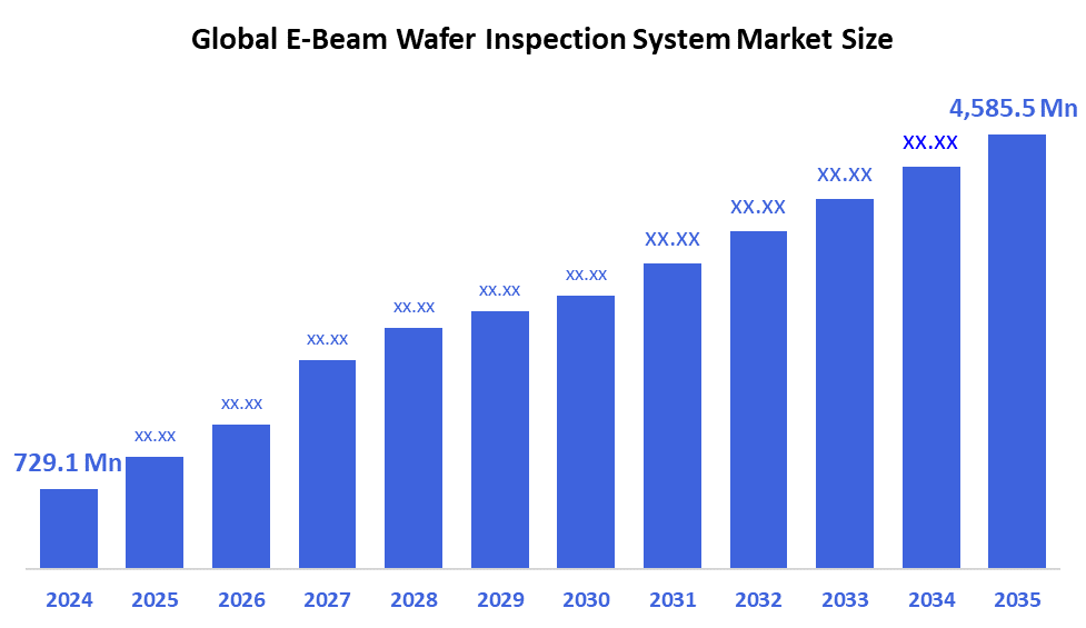
According to Spherical Insights, the Global E-Beam Wafer Inspection System Market Size is Expected to Grow from USD 729.1 Million in 2024 to USD 4,585.5 Million by 2035, at a CAGR of 18.2% during the forecast period 2025-2035. The e-beam wafer inspection system market is primarily driven by the increasing demand for precise defect detection in advanced semiconductor manufacturing with smaller feature sizes.
Key Market Insights
- Asia Pacific is expected to account for the largest share in the e-beam wafer inspection system market during the forecast period.
- In terms of wafer node, the advanced nodes (10nm, 7nm, 5nm, below) segment accounted for the largest market share of the global e-beam wafer inspection system market during the forecast period
- In terms of application, the memory chips segment accounted for the major revenue share of the global e-beam wafer inspection system market during the forecast period
Global Market Forecast and Revenue Outlook
- 2024 Market Size: USD 729.1 Million
- 2035 Projected Market Size: USD 4,585.5 Million
- CAGR (2025-2035): 18.2%
- Asia Pacific: Largest market in 2024
- Europe: Fastest growing market
E-Beam Wafer Inspection System Market
The e-beam wafer inspection system market focuses on advanced technology that uses electron beams to detect defects on semiconductor wafers, essential for manufacturing cutting-edge chips with very small feature sizes. These systems are crucial for ensuring high quality and performance in semiconductor devices, especially as traditional optical inspection methods reach their limits with newer, smaller nodes. The market is driven by increasing demand for semiconductors across industries like consumer electronics, automotive, and telecommunications. Technological advancements such as the integration of artificial intelligence and hybrid inspection methods combining electron beam and optical technologies are improving defect detection accuracy and processing speed. Government initiatives worldwide, including programs to boost domestic semiconductor manufacturing and innovation, further accelerate market growth by encouraging investment in high-precision inspection equipment. Overall, the market is poised for significant expansion due to the rising importance of semiconductor quality assurance in the evolving electronics landscape.
E-Beam Wafer Inspection System Market Trends
- Integration of AI and machine learning for enhanced defect detection accuracy and faster analysis.
- Development of hybrid inspection systems combining electron beam and optical technologies to improve throughput and resolution.
- Growing government support and investments in semiconductor manufacturing infrastructure to boost local production and innovation.
E-Beam Wafer Inspection System Market Dynamics
Driving Factors: Rising demand for high-performance chips in consumer electronics
The e-beam wafer inspection system market is growing due to the increasing complexity and miniaturization of semiconductor devices, which require more precise defect detection beyond the capabilities of traditional optical systems. Rising demand for high-performance chips in consumer electronics, automotive, and telecommunications drives the need for advanced inspection technologies. Technological advancements such as AI integration and hybrid inspection systems enhance accuracy and speed, further fueling growth. Additionally, government initiatives supporting semiconductor manufacturing and innovation encourage investments in high-precision inspection equipment, accelerating market expansion. Together, these factors contribute to robust market growth in wafer inspection technologies.
Restrain Factors: Complex technology requires specialized expertise for maintenance and operation
The growth of the e-beam wafer inspection system market is restrained by the high capital investment and operational costs associated with these advanced systems. Their complex technology requires specialized expertise for maintenance and operation, limiting accessibility for smaller manufacturers. Additionally, slower inspection speeds compared to some optical methods can impact throughput in high-volume production environments. The rapid evolution of semiconductor fabrication also demands continuous upgrades to inspection equipment, increasing overall costs. Lastly, intense competition from alternative inspection technologies and economic uncertainties in the semiconductor industry can further hinder widespread adoption and market growth.
Opportunity: Continuous push toward smaller semiconductor nodes
The e-beam wafer inspection system market presents significant opportunities driven by the continuous push toward smaller semiconductor nodes, such as 5nm and below, where traditional optical inspection falls short. The growing adoption of AI and machine learning technologies offers chances to enhance defect detection accuracy and reduce inspection time. Expanding applications in emerging sectors like automotive electronics, 5G communications, and IoT devices also open new avenues for growth. Additionally, increasing government investments and incentives worldwide aimed at strengthening semiconductor manufacturing ecosystems create favorable conditions for market expansion. Partnerships between equipment manufacturers and chipmakers to develop customized, high-throughput inspection solutions further enhance market potential. Moreover, the rise of hybrid inspection systems combining e-beam and optical techniques provides innovative ways to improve efficiency and reliability.
Challenges: Rapid advancements in semiconductor technology demand frequent upgrades
The e-beam wafer inspection system market faces challenges such as high equipment costs and complex operational requirements, which can limit adoption by smaller manufacturers. Inspection speed is slower compared to some optical systems, affecting throughput in mass production. Rapid advancements in semiconductor technology demand frequent upgrades, increasing capital expenditure. Additionally, the need for specialized technical expertise to operate and maintain these systems poses a barrier. Competition from alternative inspection technologies also adds pressure to market growth.
Global E-Beam Wafer Inspection System Market Ecosystem Analysis
The e-beam wafer inspection system market ecosystem includes key equipment manufacturers like KLA and Applied Materials, alongside semiconductor foundries such as TSMC and Renesas. Technological innovators drive advancements in AI-driven defect detection and multi-beam systems. Collaboration between manufacturers and chipmakers fuels custom solutions integrated into fabrication lines. Government initiatives, including the U.S. CHIPS Act, boost demand. Strategic partnerships and significant investments accelerate R&D in high-throughput and hybrid inspection technologies, collectively shaping market growth and innovation.
Global E-Beam Wafer Inspection System Market, By Wafer Node
The advanced nodes (10nm, 7nm, 5nm, and below) segment accounted for the largest market share of the global E-Beam Wafer Inspection System market during the forecast period, with an estimated share of approximately 22.3%. This is because, as chip manufacturers move to these smaller, more complex nodes, traditional optical inspection methods struggle to accurately detect defects due to their limited resolution. E-Beam inspection systems, with their higher precision and ability to detect extremely tiny defects, become essential for maintaining the quality and performance of these advanced chips.
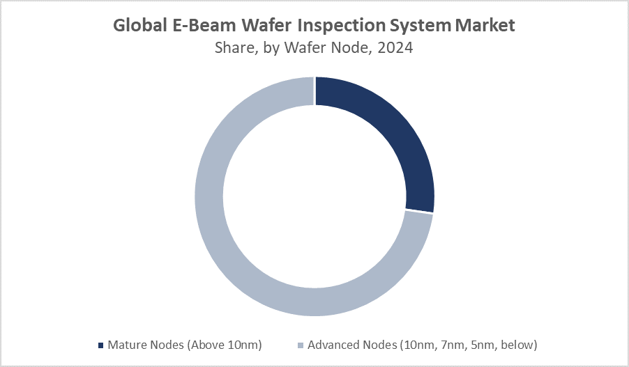
The mature nodes (above 10nm) segment accounted for a significant revenue share of the global e-beam wafer inspection system market during the forecast period, with an estimated share of over 66%. Despite the focus on cutting-edge smaller nodes, a large volume of semiconductor manufacturing still occurs at mature nodes for applications like automotive, industrial, and consumer electronics, which require reliable and cost-effective chips. E-Beam inspection systems are widely used in these mature processes to ensure high yield and quality, driving substantial market revenue from this segment.
Global E-Beam Wafer Inspection System Market, By Application
The memory chips segment held an estimated 34% of the total market revenue during the forecast period, accounting for the major revenue share of the global e?beam wafer inspection system market. This is because memory chip manufacturing, including DRAM and NAND flash, demands extremely precise defect inspection to ensure reliability and performance. As memory technologies advance and densities increase, the need for high-resolution inspection methods like E-Beam systems grows, driving significant adoption and revenue within this segment.
The logic chips segment accounted for a substantial revenue share of the global e?beam wafer inspection system market during the forecast period, holding an estimated market share of approximately 25%. Logic chip manufacturing involves complex and highly integrated circuits that require precise defect detection to maintain performance and yield. As demand for advanced processors and system-on-chips (SoCs) grows, E-Beam inspection systems play a crucial role in ensuring the quality of these devices, contributing significantly to the market’s revenue within this segment.
Asia Pacific region accounted for the largest share of the e-beam wafer inspection system market, with an estimated market share of around 40%.
This dominance is driven by the region’s strong semiconductor manufacturing base, led by countries like China, Taiwan, South Korea, and Japan. With major foundries and chipmakers investing heavily in advanced technology nodes and wafer inspection equipment, Asia Pacific continues to be the primary hub for semiconductor production and innovation, fueling significant demand for E-Beam inspection systems.
China is the fastest-growing country in the Asia Pacific e-beam wafer inspection system market, with an estimated regional market share of approximately 18%.
This rapid growth is fueled by substantial government investments in semiconductor manufacturing, efforts to build a self-reliant chip industry, and increasing demand for advanced inspection technologies. China’s expanding fabrication facilities and focus on cutting-edge semiconductor technologies are driving strong adoption of E-Beam inspection systems, making it a key growth engine in the region.
Europe is projected to be the fastest-growing region in the global e-beam wafer inspection system market during the forecast period, with an estimated market share of approximately 25.7%.
This growth is driven by significant government initiatives like the European Chips Act, aimed at boosting semiconductor manufacturing and innovation within the region. Increasing investments in local fabs, advanced research, and collaborations between industry players are fueling demand for high-precision inspection technologies such as E-Beam systems, positioning Europe as a rapidly expanding market.
WORLDWIDE TOP KEY PLAYERS IN THE E-BEAM WAFER INSPECTION SYSTEM MARKET INCLUDE
- ASML Holding NV
- Applied Materials, Inc.
- KLA Corporation
- Hitachi High-Technologies Corporation
- JEOL Ltd.
- Nikon Corporation
- Canon Inc.
- Cognex Corporation
- ViTrox Corporation Berhad
- Lasertec Corporation
- Others
Product Launches in E-Beam Wafer Inspection System Market
- In December 2024, Tokyo Seimitsu announced a strategic collaboration with a leading semiconductor manufacturer to develop next-generation e-beam inspection technologies. The primary objective of this partnership is to reduce defect detection times by 25%, thereby enhancing the efficiency and accuracy of semiconductor manufacturing processes.
Market Segment
This study forecasts revenue at global, regional, and country levels from 2020 to 2035. Decision Advisors has segmented the e-beam wafer inspection system market based on the below-mentioned segments:
Global E-Beam Wafer Inspection System Market, By Wafer Node
- Mature Nodes (Above 10nm)
- Advanced Nodes (10nm, 7nm, 5nm, below)
Global E-Beam Wafer Inspection System Market, By Application
- Logic Chips
- Memory Chips
Global E-Beam Wafer Inspection System Market, By Regional Analysis
- North America
- US
- Canada
- Mexico
- Europe
- Germany
- UK
- France
- Italy
- Spain
- Russia
- Rest of Europe
- Asia Pacific
- China
- Japan
- India
- South Korea
- Australia
- Rest of Asia Pacific
- South America
- Brazil
- Argentina
- Rest of South America
- Middle East & Africa
- UAE
- Saudi Arabia
- Qatar
- South Africa
- Rest of the Middle East & Africa
FAQs
Q: What wafer node segment accounts for the largest market share?
A: The advanced nodes segment (10nm, 7nm, 5nm, and below) accounted for the largest market share during the forecast period.
Q: Which application segment dominates the Global E-Beam Wafer Inspection System Market?
A: The memory chips segment accounted for the major revenue share of the market during the forecast period.
Q: Who are the key players in the Global E-Beam Wafer Inspection System Market?
A: Top companies include ASML Holding NV, Applied Materials, Inc., KLA Corporation, Hitachi High-Technologies Corporation, JEOL Ltd., Nikon Corporation, Canon Inc., Cognex Corporation, ViTrox Corporation Berhad, and Lasertec Corporation.
Q: What are the main drivers of growth in the E-Beam Wafer Inspection System Market?
A: Rising demand for precise defect detection in advanced semiconductor manufacturing, increased semiconductor demand across industries, technological advancements including AI integration, and government initiatives supporting semiconductor manufacturing are the main growth drivers.
Q: What challenges are limiting the adoption of E-Beam Wafer Inspection Systems?
A: High capital and operational costs, requirement for specialized expertise, slower inspection speeds compared to some optical methods, and frequent equipment upgrades due to rapid semiconductor technology advancements are key challenges.
Q: What emerging trends are shaping the E-Beam Wafer Inspection System Market?
A: Integration of AI and machine learning for enhanced defect detection, development of hybrid inspection systems combining electron beam and optical technologies, and growing government investments in semiconductor infrastructure are major trends.
Q: What are the key opportunities in the Global E-Beam Wafer Inspection System Market?
A: Opportunities include the continuous push toward smaller semiconductor nodes (5nm and below), expansion in automotive electronics, 5G, IoT sectors, government incentives, and partnerships between equipment manufacturers and chipmakers for customized high-throughput solutions.
Q: How does Asia Pacific compare to other regions in terms of market size and growth?
A: Asia Pacific holds the largest market share (around 40%) driven by strong semiconductor manufacturing bases in China, Taiwan, South Korea, and Japan. China is the fastest-growing country in this region due to government investments and expanding fabrication facilities.
Q: What is the role of advanced nodes in the E-Beam Wafer Inspection System Market?
A: Advanced nodes require higher precision defect detection that traditional optical methods cannot provide, making E-Beam inspection systems essential for maintaining quality and performance of chips at these smaller feature sizes.
Q: What are some recent developments or product launches in the market?
A: In December 2024, Tokyo Seimitsu announced a strategic collaboration to develop next-generation e-beam inspection technologies aimed at reducing defect detection times by 25%.
Q: Which application segments are expected to see significant growth?
A: Both memory chips and logic chips segments are growing, with memory chips accounting for 34% of market revenue and logic chips for approximately 25% due to increasing demand for high-performance semiconductor devices
Check Licence
Choose the plan that fits you best: Single User, Multi-User, or Enterprise solutions tailored for your needs.
We Have You Covered
- 24/7 Analyst Support
- Clients Across the Globe
- Tailored Insights
- Technology Tracking
- Competitive Intelligence
- Custom Research
- Syndicated Market Studies
- Market Overview
- Market Segmentation
- Growth Drivers
- Market Opportunities
- Regulatory Insights
- Innovation & Sustainability
Report Details
| Scope | Global |
| Pages | 250 |
| Delivery | PDF & Excel via Email |
| Language | English |
| Release | May 2025 |
| Access | Download from this page |