Global Optical Patterned Wafer Inspection Equipment (OPWIE) Market
Global Optical Patterned Wafer Inspection Equipment (OPWIE) Market Size, Share, and COVID-19 Impact Analysis, By Type of Inspection (Critical Dimension Measurement, Defect Detection), By Technology (Optical Inspection and Electron Beam Inspection), By End-User Industry (Semiconductor Manufacturing and Consumer Electronics), By Automation Level (Fully Automatic, Semi-Automatic), By Wafer Size (200 mm Wafer, 300 mm Wafer), and By Region (North America, Europe, Asia-Pacific, Latin America, Middle East, and Africa), Analysis and Forecast 2023 - 2033
Report Overview
Table of Contents
Global Optical Patterned Wafer Inspection Equipment (OPWIE) Market Overview
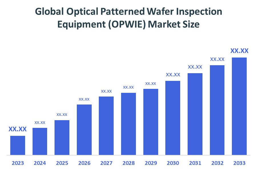
- The Global Optical Patterned Wafer Inspection Equipment (OPWIE) Market Size is Anticipated to Exceed USD 7.72 Billion by 2033, growing at a CAGR of 17.04% from 2023 to 2033.
- The market growth is rising due to the rising demand for high-performance semiconductors and the continuous miniaturization of electronic devices.
- As chip designs become more complex, manufacturers require advanced inspection tools to detect defects with greater accuracy and speed. Additionally, the increasing adoption of automation and artificial intelligence in semiconductor fabrication enhances the need for precise inspection systems like OPWIE.
- The growing investment in semiconductor foundries and the expansion of 5G, IoT, and AI technologies are further propelling market demand.
Major vendors in the Global Optical Patterned Wafer Inspection Equipment (OPWIE) Market
Hermes Microvision, KLA-Tencor, Applied Materials, Hitachi High-Technologies, ASML, Tokyo Seimitsu, Toray Engineering, JEOL, and Tokyo Seimitsu, and others.
Market Segment
This study forecasts revenue at global, regional, and country levels from 2023 to 2033. Decision Advisor has segmented the optical patterned wafer inspection equipment (OPWIE) market based on the below-mentioned segments:
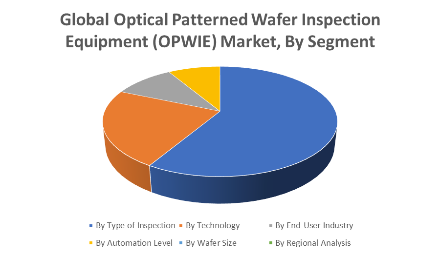
Global Optical Patterned Wafer Inspection Equipment (OPWIE) Market, By Type of Inspection
- Critical Dimension Measurement
- Defect Detection
Global Optical Patterned Wafer Inspection Equipment (OPWIE) Market, By Technology
- Optical Inspection
- Electron Beam Inspection
Global Optical Patterned Wafer Inspection Equipment (OPWIE) Market, By End-User Industry
- Semiconductor Manufacturing
- Consumer Electronics
Global Optical Patterned Wafer Inspection Equipment (OPWIE) Market, By Automation Level
- Fully Automatic
- Semi-Automatic
Global Optical Patterned Wafer Inspection Equipment (OPWIE) Market, By Wafer Size
- 200 mm Wafer
- 300 mm Wafer
Global Optical Patterned Wafer Inspection Equipment (OPWIE) Market, By Regional Analysis
- North America
- US
- Canada
- Mexico
- Europe
- Germany
- UK
- France
- Italy
- Spain
- Russia
- Rest of Europe
- Asia Pacific
- China
- Japan
- India
- South Korea
- Australia
- Rest of Asia Pacific
- South America
- Brazil
- Argentina
- Rest of South America
- Middle East & Africa
- UAE
- Saudi Arabia
- Qatar
- South Africa
- Rest of the Middle East & Africa
Check Licence
Choose the plan that fits you best: Single User, Multi-User, or Enterprise solutions tailored for your needs.
We Have You Covered
- 24/7 Analyst Support
- Clients Across the Globe
- Tailored Insights
- Technology Tracking
- Competitive Intelligence
- Custom Research
- Syndicated Market Studies
- Market Overview
- Market Segmentation
- Growth Drivers
- Market Opportunities
- Regulatory Insights
- Innovation & Sustainability
Report Details
| Scope | Global |
| Pages | 250 |
| Delivery | PDF & Excel via Email |
| Language | English |
| Release | Sep 2025 |
| Access | Download from this page |