Global Semiconductor Assembly & Packaging Equipment Market
Global Semiconductor Assembly & Packaging Equipment Market Size, Share, and COVID-19 Impact Analysis, By Product (Dicing Equipment, Bonding Equipment, Packaging Equipment, Others), By Packaging Type (Flip Chip Packaging Equipment, Wafer Level Packaging (WLP) Equipment, Fan-Out Packaging Equipment, System-in-Package (SiP) Equipment, 3D/2.5D Packaging Equipment, Others), and By Region (North America, Europe, Asia-Pacific, Latin America, Middle East, and Africa), Analysis and Forecast 2025 - 2035.
Report Overview
Table of Contents
Semiconductor Assembly & Packaging Equipment Market Summary
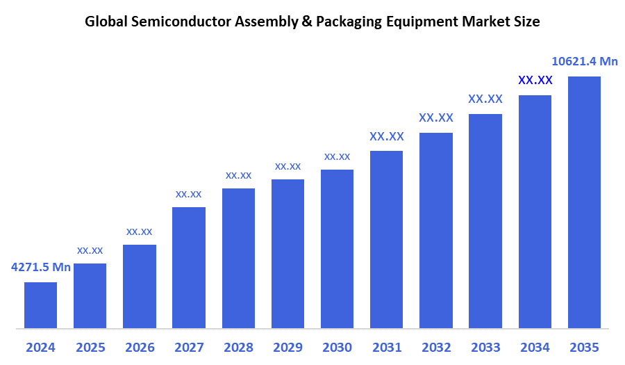
The Global Semiconductor Assembly and Packaging Equipment Market Size Was Estimated at USD 4271.5 Million in 2024 and is Projected to Reach USD 10621.4 Million by 2035, Growing at a CAGR of 8.63% from 2025 to 2035. The market for semiconductor assembly and packaging equipment is expanding due to factors such as the growing need for small, high-performing devices, the development of 5G and AI technologies, the growing use of IoT, and the move toward sophisticated packaging.
Key Regional and Segment-Wise Insights
- In 2024, the Asia Pacific held the largest revenue share of over 66.4% and dominated the market globally.
- In 2024, the bonding equipment segment had the highest market share by product, accounting for 33.2%.
- In 2024, the fixed roof segment had the biggest market share by packaging type, accounting for 29.5%.
Global Market Forecast and Revenue Outlook
- 2024 Market Size: USD 4271.5 Million
- 2035 Projected Market Size: USD 10621.4 Million
- CAGR (2025-2035): 8.63%
- Asia Pacific: Largest market in 2024
The Semiconductor Assembly & Packing Equipment Market refers to the industry that manufactures equipment used for assembling and packing semiconductor devices, including die bonding, wire bonding, flip-chip, and wafer-level packaging processes. The market transforms silicon wafers into operational chips that electronic devices can integrate, thus positioning itself as an essential part of the semiconductor value chain. The main growth factors include the expanding adoption of AI alongside IoT and 5G technologies, together with the fast expansion of smart devices and automotive electronics. The market experiences growth because of rising demand for advanced packaging solutions, which stems from the current trend of shrinking device size and growing chip complexity.
The semiconductor assembly and packaging equipment market experiences a substantial transformation because of technological advancements. The latest developments, including fan-out wafer-level packaging together with system-in-package (SiP), alongside 3D packaging, enable greater integration alongside enhanced performance with decreased power consumption. Equipment manufacturers focus on automating their processes while enhancing accuracy and scaling capabilities because of increasing production needs. Various governments across the globe, specifically the United States, South Korea, Taiwan, and European Union member states, invest heavily in developing their own semiconductor supply chains through financial incentives combined with research and development funding. Through these initiatives, the market expands over time as industrial capabilities within local regions become stronger.
Product Insights

What Factors Enabled the Bonding Equipment Segment to Capture a 33.2% Revenue Share in the Semiconductor Assembly & Packaging Equipment Market in 2024?
The bonding equipment segment led the Semiconductor Assembly & Packaging Equipment market with the largest revenue share of 33.2% in 2024. The essential role of bonding equipment in semiconductor packaging operations, which include wire bonding and die bonding, and flip-chip bonding, accounts for its dominant market position. These procedures represent vital steps for generating electrical connections between semiconductor devices because they deliver performance alongside dependability and enable the reduction of device sizes. Sophisticated bonding solutions become essential because semiconductor chip complexity rises and high-density packaging requirements emerge. The growing demand for this equipment stems from its expanding use in automotive and telecommunications applications as well as consumer electronics. This area secures its market leadership status through ongoing developments that enhance bonding precision and automation, together with increased processing speed.
The packaging equipment segment of the semiconductor assembly & packaging equipment market is expected to grow at the fastest CAGR throughout the forecast period. Packaging equipment needs for improved performance and smaller size, along with enhanced power efficiency, such as 3D packaging and system-in-package (SiP) and fan-out wafer-level packaging, drive rapid market growth. Packaging equipment plays a vital role in protecting chips while enabling high-density integration of modern, sophisticated semiconductor devices, which continue to shrink in size. The demand for advanced packaging technologies continues to rise because new applications in 5G, AI, IoT, and automotive electronics have appeared. The packaging equipment market category remains at the forefront of the semiconductor assembly and packaging industry because of continuous improvements in automation systems and material precision, and packaging technologies.
Packaging Type Insights
How Did Wafer-Level Packaging Equipment Emerge as the Leading Packaging Type Segment in 2024?
The wafer-level packaging equipment segment led the semiconductor assembly & packaging equipment market with 29.5% revenue share in 2024. The growing adoption of wafer-level packaging (WLP) technology leads the market because WLP delivers smaller package sizes and better electrical performance at lower production costs. The applications that require compact dimensions mainly choose WLP technology for their packaging needs, including wearables and smartphones, and Internet of Things devices. The expanding need for compact high-performance semiconductor devices drives this market forward. The market growth receives additional support from WLP technology advancements, including fan-out wafer-level packaging (FOWLP), which enhances both package density and heat management capabilities. Semiconductor manufacturers worldwide continue to prioritize wafer-level packaging equipment because of its efficient, scalable properties.
The 3D/2.5D packaging equipment segment of the semiconductor assembly & packaging equipment market is anticipated to grow at the fastest CAGR during the projected period. Advanced packaging solutions, which enhance semiconductor device performance while reducing power consumption, drive this rapid growth. The vertical stacking of multiple chips using 3D and 2.5D packaging methods enables higher chip density along with lower latency, which proves essential for advanced applications, including artificial intelligence and data centers, and 5G networks. The implementation rate of small multipurpose devices for both consumer electronics and automotive sectors drives faster adoption of this technology. Through-silicon vias (TSVs) alongside interposers have enabled new opportunities for 3D/2.5D packaging, which drives the fastest expansion of this market segment.
Regional Insights
The North American semiconductor assembly and packaging equipment market accounted for significant growth because modern semiconductor devices receive high demand from consumer electronics applications and automotive systems and aerospace, and healthcare industries. Regional semiconductor manufacturing facilities benefit from substantial support provided by leading technology providers and equipment manufacturers. Large-scale R&D investments, along with government programs dedicated to expanding semiconductor manufacturing within domestic borders, create market growth opportunities. The market experiences growth due to rising interest in sophisticated packaging methods, which include wafer-level and 3D packaging technologies. The rising focus on automated semiconductor assembly with precise methods drives production efficiency while creating an explosive market growth trend in North America.
Europe Semiconductor Assembly and Packaging Equipment Market Trends
The market for semiconductor assembly and packaging equipment in Europe experiences continuous growth because of its focus on production sophistication and innovation, along with stringent quality standards. The European market experiences high demand for advanced packaging and assembly equipment because of its substantial automotive and aerospace, and industrial sectors, which consume semiconductor devices extensively. The European Union's Chips Act, along with other government initiatives, backs semiconductor research and development investments to improve local chip production and minimize foreign dependency. Advanced packaging solutions, such as 3D and wafer-level packaging experiencing rising adoption rates, which drives market expansion. The European market will sustain its growth throughout the forecast period because of increasing interest in sustainable manufacturing practices and energy-efficient production methods.
Asia Pacific Semiconductor Assembly and Packaging Equipment Market Trends
In 2024, the Asia Pacific region held the largest revenue share of 66.4% and dominated the worldwide semiconductor assembly and packaging equipment market. The leading position of this region stems from its established semiconductor production centers in China and Taiwan as well as South Korea, and Japan. The area benefits from its extensive manufacturing facilities, together with skilled laborers and a well-developed supply chain network. Rapid development in consumer electronics and automotive electronics, and telecommunications sectors drives the need for advanced packaging solutions. The market expands because public and private organizations allocate substantial funds to boost semiconductor manufacturing capabilities and adopt state-of-the-art technology. The growing use of 5G, AI, and IoT applications establishes Asia Pacific as the leading market for advanced assembly and packaging equipment worldwide.
Key Semiconductor Assembly And Packaging Equipment Companies:
The following are the leading companies in the semiconductor assembly and packaging equipment market. These companies collectively hold the largest market share and dictate industry trends.
- Applied Materials
- Teradyne, Inc.
- Plasma-Therm
- ASM Pacific Technology
- Rudolph Technologies, Inc.
- Disco Corporation
- SUSS MicroTec SE
- Tokyo Electron Limited (TEL)
- Besi
- Nikon Corporation
- Veeco Instruments Inc.
- Lam Research Corporation
- Ultratech, Inc.
- Others
Recent Developments
- In May 2025, Veeco announced that both IDMs and OSATs have placed orders totaling more than USD 35 million for their AP300 advanced packaging lithography systems. These systems will help meet the growing need for production linked to the markets for AI and high-performance computing. The AP300 is best suited for fan-out wafer-level packing, flip chip, and copper pillar bumping. It is anticipated that this increase in orders would greatly bolster Veeco's advanced packaging equipment business in 2025.
- In August 2024, an Indian opto-semiconductor company entitled Polymatech, purchased the American Nisene Technology Group to increase its footprint in IC testing and packaging. In doing so, Polymatech advances its objective of creating a complete semiconductor ecosystem. Plans to expand operations in the United States through significant investment are also included. Through this acquisition, the company's capabilities are enhanced throughout the value chain of chipmaking.
Market Segment
This study forecasts revenue at global, regional, and country levels from 2020 to 2035. Decision Advisor has segmented the semiconductor assembly & packaging equipment market based on the below-mentioned segments:
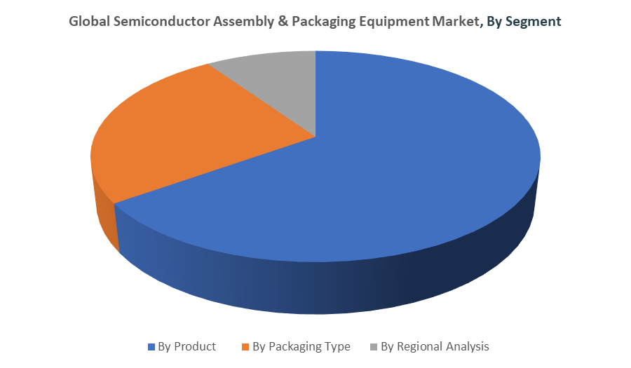
Global Semiconductor Assembly & Packaging Equipment Market, By Product
- Dicing Equipment
- Bonding Equipment
- Packaging Equipment
- Others
Global Semiconductor Assembly & Packaging Equipment Market, By Packaging Type
- Flip Chip Packaging Equipment
- Wafer Level Packaging (WLP) Equipment
- Fan-Out Packaging Equipment
- System-in-Package (SiP) Equipment
- 3D/2.5D Packaging Equipment
- Others
Global Semiconductor Assembly & Packaging Equipment Market, By Regional Analysis
- North America
- US
- Canada
- Mexico
- Europe
- Germany
- UK
- France
- Italy
- Spain
- Russia
- Rest of Europe
- Asia Pacific
- China
- Japan
- India
- South Korea
- Australia
- Rest of Asia Pacific
- South America
- Brazil
- Argentina
- Rest of South America
- Middle East & Africa
- UAE
- Saudi Arabia
- Qatar
- South Africa
- Rest of the Middle East & Africa
Check Licence
Choose the plan that fits you best: Single User, Multi-User, or Enterprise solutions tailored for your needs.
We Have You Covered
- 24/7 Analyst Support
- Clients Across the Globe
- Tailored Insights
- Technology Tracking
- Competitive Intelligence
- Custom Research
- Syndicated Market Studies
- Market Overview
- Market Segmentation
- Growth Drivers
- Market Opportunities
- Regulatory Insights
- Innovation & Sustainability
Report Details
| Scope | Global |
| Pages | 236 |
| Delivery | PDF & Excel via Email |
| Language | English |
| Release | Sep 2025 |
| Access | Download from this page |