Global Semiconductor Dry Strip Systems Market
Global Semiconductor Dry Strip Systems Market Size, Share, By Type (Remote Plasma, Inductively Coupled Plasma) By Application (Logic, Memory, Foundry, and Others) By Technology Node (7nm & below, 10-28nm, Above 28nm) and By Region (North America, Europe, Asia-Pacific, Latin America, Middle East and Africa), Analysis and Forecast 2026 - 2035
CAGR
4.18%
REVENUE 2025
USD Million 390.2
FORECAST 2035
USD Million 587.4
REPORT COVERAGE
Global
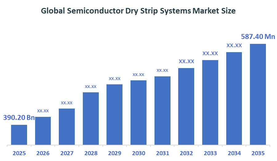
The Global Semiconductor Dry Strip Systems Market Size was predicted to grow from USD 390.20 Million in 2025 and is projected to reach around USD 587.40 Million by 2035. According to Decision Advisors, a detailed research report on the semiconductor dry strip systems market shows that the Remote Plasma segment dominates the global semiconductor dry strip systems market, holding approximately 55-60% of the total share worldwide. Lam Research leads the market with approximately with total annual revenue reaching $20.6 billion in 2025, making it one of the major market drivers for shaping the industry.
Market Snapshot
- Global Semiconductor Dry Strip Systems Market Size (2025): USD 390.20 Million
- Global Semiconductor Dry Strip Systems Projected Market Size (2035): USD 587.40 Million
- Global Semiconductor Dry Strip Systems Compound Annual Growth Rate (CAGR): 4.18%
- Largest Regional Market: Asia-Pacific
- Fastest Growing Region: North America
- 3rd Largest Region: Europe
- Base Year: 2025
- Historical Period: 2021 - 2024
- Forecast Period: 2026 - 2035
Market Overview / Introduction
The dry strip systems are a collection of parts that create plasma and enable the removal of photoresists and organic matter on silicon wafers. The dry strip systems play important roles in connecting processes of lithography and following processes of etching and ion implantation, employing plasma chemistry and technology in such a way that the highest level of purity will be achieved at minimum usage time. There are several features that characterise today's dry strip systems, including selectivity and low damage processes. The dry strip systems have come a long way from basic oxygen ashers to high-tech plasma systems that are made up of radical sources and heat-resistant capabilities while operating in dense 3D NAND and logic production. Such an increase in usage has resulted from the rising demand for high-node chips and vertical transistor manufacturing in technologically progressing areas and data centers. The dry strip systems have become a necessity due to their ability to safeguard the semiconductor devices against loss of performance through the presence of chemicals in the production process without using any chemical solvents.
- The foundry and memory segments contribute to approximately 62% of the application-based use in the market, driven by the increasing demand for AI-specific chips, high-bandwidth memory (HBM), and the maintenance of advanced logic production lines.
- There is an exponential rise in the development of low-damage remote plasma systems in the foundry industry, and the CAGR is predicted to exceed 6.8% because of the growing application of gate-all-around (GAA) transistors in next-generation processors due to their ability to offer optimized switching and efficiency.
Notable Insights: -
- Remote plasma stripping modules make up about 55-60% of the total market share of this sector.
- Applications of dry strip systems in the sphere of 3D semiconductor architectures account for almost 41% of all demand.
- Multi-chamber dry strip systems show an annual increase above 5.9%.
What is the Role of Technology in Shaping the Market?
There have been several improvements in technology that have greatly impacted the field of stripping in terms of stripping efficiency, process selectivity, and surface integrity of the wafer surface. The latest dry strip technology has transcended from being used just as a means of removing photoresist to plasma systems capable of working in a high vacuum environment due to their ability to perform in pulse mode using microwaves and Faraday shields.
How are Recent Developments Helping the Market?
These include the adoption of cryogenic wafer cooling technology, advanced endpoint detectors, and metrology systems. These innovations have been very instrumental in promoting the growth and development of the market. Innovations have occurred whereby there is the production of tools which can effectively withstand pattern leaning while protecting all kinds of high aspect ratio structures, such as those utilised in the production of mobile processors, as well as those used in servers. This innovation will enable the production of dense circuitry through the utilisation of chemical processes in current-day plasma sources without physical sputtering or breakdown.
Market Drivers
The demand for global semiconductor dry strip systems is increasing due to increasing investment by major players and governments in domestic chip production and advanced node development to cater to AI and 5G needs in the present era. Modern dry strip systems have gained immense popularity in the market due to their ability to incorporate several characteristics within a single robust system, including minimal silicon wastage, high ashing ratio, and particle control. At the same time, the emergence of mega-fabs has resulted in an increased need for automation of the stripping process to cater to the evolving trend of moving from batch-wise operations to high-volume single-wafer chambers with improved plasma control.
Restraints
Nevertheless, the expansion of the international market for the semiconductor dry strip sector is hindered by the difficulties in ensuring the consistency of the supply chain of specialty gases and high-purity quartz material, taking into account that the international market can be volatile and may create issues related to lead time.
Competitive Analysis:
The report offers the appropriate analysis of the key organisations/companies involved within the semiconductor dry strip systems market, along with a comparative evaluation primarily based on their product offerings, business overviews, geographic presence, enterprise strategies, segment market share, and SWOT analysis. The report also provides an elaborate analysis focusing on the current news and developments of the companies, which includes product development, innovations, joint ventures, partnerships, mergers & acquisitions, strategic alliances, and others. This allows for the evaluation of the overall competition within the market.
Top 10 Companies in the Global Semiconductor Dry Strip Systems Market
- Lam Research Corporation
- Applied Materials, Inc.
- Tokyo Electron Limited (TEL)
- Entegris (Versum Materials)
- Mattson Technology, Inc.
- Hitachi High-Tech Corporation
- GigaLane
- PSK Inc.
- Ulvac, Inc.
- Plasma-Therm
Government Initiatives
|
Country |
Key Government Initiatives |
|
US |
The Manufacturing USA Program Strategic Plan (2026-2030), published in March 2026, outlines a vision for US global leadership in advanced manufacturing. The plan focuses on transitioning innovative technologies into scalable domestic capabilities with a strategic investment strategy designed to secure the supply chain for high-precision machine tools used in national defense and aerospace. |
|
India |
The Samarth Udyog Bharat 4.0 initiative and the Union Budget 2026-27 have reinforced manufacturing as a core economic pillar. The government has introduced a ?10,000 crore SME Growth Fund and mandates a Phased Manufacturing Programme (PMP) to increase the manufacturing sector’s GVA, which saw a 9.13% growth in late 2025, encouraging the upgrade of traditional slotting machines to IoT-enabled units. |
|
Germany |
The Industrie 4.0 Strategy remains a global benchmark, with 2026 data showing that 71% of German manufacturing companies have now adopted Industry 4.0 technologies. The government has allocated significant research funding including USD 300 million in regional digital hubs like Stuttgart to advance AI-driven manufacturing and predictive maintenance in high-end precision machinery. |
Study on the Supply, Demand, Distribution, and Market Environment
For the semiconductor dry strip systems market, it is crucial to find an equilibrium between operating at peak throughput and higher selectivity needs that must be achieved without compromising effectiveness and damaging potential. Dry strip systems are produced using cutting-edge RF generators and ceramic parts, which provide continuous plasma stability while eliminating metal contamination associated with outdated semiconductor dry strip tools.
Price Analysis and Consumer Behaviour Analysis
Systems' costs will depend on how many chambers there are, the complexity of the plasma generator, and the degree of automation in wafer handling processes. The most complex setups, which are meant for 5 nm devices and smaller, are costly due to the presence of sensors and high-frequency power sources. In contrast, older dry stripper systems for power semiconductors and analogue ICs are cheap and present good opportunities for regional manufacturers and research labs. People are interested in systems with high uptime and few defects, meaning that companies must strive to manufacture durable and easily upgradeable systems.
Market Segmentation
The Global Semiconductor Dry Strip Systems Market share is classified into type, application, and technology node.
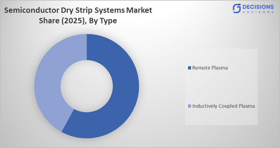
The Remote Plasma segment holds the largest share, contributing approximately 55-60% of the market in 2025.
Based on the Type, the global semiconductor dry strip systems market is divided into Remote Plasma and Inductively Coupled Plasma. Among these, the Remote Plasma segment holds the largest share, contributing approximately 55-60% of the market in 2025. The justification behind this is the fact that these products are capable of functioning more efficiently in terms of low-damage chemical stripping at high throughput rates, as well as the ability of these materials to withstand high-volume processing while using minimal ion bombardment in comparison to the normal direct plasma sources used. The second group of products comprises the inductively coupled plasma systems.
Foundry dominates the global market, accounting for approximately 45% of the total revenue in 2025.
Based on the Application, the global semiconductor dry strip systems market is divided into Logic, Memory, Foundry, and Others. Among these, Foundry dominates the global market, accounting for approximately 45% of the total revenue in 2025. The justification behind this is the fact that these facilities are capable of functioning more efficiently in terms of manufacturing a variety of chip designs at fast production rates, as well as the ability of these foundries to offer specialized stripping services while using minimal turnaround time in comparison to the captive fab models used. The second group of applications comprises the memory segment.
The 7nm & Below segment accounts for the largest share, representing over 40% of the global market in 2025.
Based on the Technology Node, the global semiconductor dry strip systems market is divided into 7nm & below, 10-28nm, and Above 28nm. Among these, the 7nm & Below segment accounts for the largest share, representing over 40% of the global market in 2025. The justification behind this is the fact that these systems are critical for leading-edge logic and memory, providing the precision required for complex 3D structures at fast production rates, as well as the ability of these tools to maintain substrate integrity while using minimal material loss in comparison to the legacy nodes used. The second group of nodes comprises the 10-28nm segment.
Strategies to Implement for Growth of the Market in Non-Leading Regions
The possibilities of growth for the semiconductor dry strip industry in emerging regions can be enhanced through the creation of efficient localized service centers for the use of regional fab operators, as well as local bodies responsible for managing the expansion of electronics manufacturing. The initiatives from the government focused on chip sovereignty, together with an increase in the manufacture of legacy node chips, play a major role in creating a demand in those regions that face difficulties regarding the importation of high-end equipment. The additional assistance of investment in the training of local plasma physics engineers, together with regional hardware support labs, will help achieve this.
Regional Segment Analysis of the Global Semiconductor Dry Strip Systems Market
- North America (U.S., Canada, Mexico)
- Europe (Germany, France, U.K., Italy, Spain, Rest of Europe)
- Asia-Pacific (China, Japan, India, South Korea, Rest of APAC)
- Latin America (Brazil and the Rest of Latin America)
- The Middle East and Africa (UAE, South Africa, Rest of MEA)
Asia-Pacific is projected to be the largest region over the forecast period. This region is anticipated to witness a growth rate of around 6.45% CAGR, maintaining a dominant market share within the global industry. In 2025, the Asia-Pacific region will already account for approximately 58% of global revenue. This is owing to the massive concentration of foundries and IDMs in countries such as Taiwan, South Korea, and China. Other reasons for the same include greater investments made toward fab capacity expansion in the region, state-supported indigenous manufacturing projects for semiconductor equipment, and widespread adoption of 3D packaging standards.
North America is expected to hold a significant share of the semiconductor dry strip systems market during the forecast period. This region holds approximately 20% share of global revenue in 2025, thanks to its leading position in logic design, along with the extensive adoption of AI-driven equipment in national semiconductor programs and high-value industrial applications. The largest part of this region’s revenues comes from the United States, as there is a lot of spending at the corporate level in modernization programs for advanced fabs, along with local research related to next-generation plasma sources.
Europe is anticipated to hold a substantial share, contributing approximately 15% of the global market share. There is a competitive advantage in the region owing to clusters of semiconductor research centers and financing for sustainable digital transitions, as well as equipment efficiency research. There is also a comparative advantage with countries like Germany and the Netherlands, which are highly skilled at precision engineering for lithography-adjacent tools. Moreover, the rigorous industrial standards regarding process safety and material waste further give them a competitive advantage.
Recent Developments
- In March 2026, Tokyo Electron (TEL) celebrated the fifth anniversary of its E-COMPASS initiative, a collaborative supply chain program focused on reducing the environmental impact of semiconductor equipment. This initiative involves partnerships with over 500 business entities to innovate low-power plasma stripping and etching solutions for the green society transition.
- In May 2024, Mattson Technology expanded its SUPREMA product family, launching a new generation of high-productivity plasma dry strip systems. The system features a unique twin-wafer chamber design with an Inductively Coupled Plasma (ICP) source and a grounded Faraday shield, specifically designed to eliminate masking layers from wafers without damaging surface materials at advanced nodes.
- In June 2023, Lam Research initiated a comprehensive Collaborative Spare Parts Program aimed at enhancing cost efficiency and sustainability for global chipmakers.
- In November 2021, Hitachi High-Tech introduced a hybrid plasma-laser hybrid system designed to improve the welding and processing efficiency of copper-based semiconductor components. This breakthrough reduces manufacturing power consumption by nearly 30% compared to legacy stripping and welding systems.
Market Segmentation
This study forecasts revenue at global, regional, and country levels from 2021 to 2035. The Global Semiconductor Dry Strip Systems Market is segmented based on the following categories:
Global Semiconductor Dry Strip Systems Market, By Type:
- Remote Plasma
- Inductively Coupled Plasma
Global Semiconductor Dry Strip Systems Market, By Technology Node:
- 7nm & Below
- 10-28nm
- Above 28nm
Global Semiconductor Dry Strip Systems Market, By Application:
- Logic
- Memory
- Foundry
- Others
Global Semiconductor Dry Strip Systems Market, By Regional Analysis:
- North America
- United States
- Canada
- Mexico
- Europe
- Germany
- United Kingdom
- France
- Italy
- Spain
- Russia
- Rest of Europe
- Asia Pacific
- China
- Japan
- India
- South Korea
- Australia
- Rest of Asia Pacific
- Latin America
- Brazil
- Argentina
- Rest of Latin America
- Middle East & Africa
- United Arab Emirates
- Saudi Arabia
- Qatar
- South Africa
- Rest of Middle East & Africa
Frequently Asked Questions (FAQ)
What is the significance of low-damage stripping in modern semiconductor fabrication?
Advanced nodes utilize delicate materials and 3D architectures that are sensitive to ion impact and charging. Low-damage stripping, often achieved via remote plasma sources, ensures that the photoresist is removed without eroding the silicon or causing dielectric breakdown. This technique is necessary for extending the reliability of transistors in high-speed processors and mobile devices.
How does the transition to 3D GAAFET architectures affect dry strip specifications?
The adoption of Gate-All-Around (GAA) structures increases the surface area that must be cleaned. This requires stripping processes with exceptionally high lateral etch rates and selectivity to prevent the collapse of the vertical nanosheets. One solution is the use of specialized hydrogen-based chemistries that prevent oxidation of the silicon surface.
What role does integrated metrology play in high-performance dry strip systems?
Integrated metrology allows for real-time monitoring of the stripping rate and endpoint detection. In manufacturing environments where wafer costs are high, this offers the necessary precision to avoid over-stripping, ensuring the integrity of the underlying layers during rapid production cycles.
What are the primary differences in the application of remote versus direct plasma stripping in 2026?
While direct plasma is still used for bulk stripping where speed is the priority, remote plasma is seeing increased adoption for critical layers. Remote plasma's significantly lower ion energy makes it ideal for charge-sensitive devices where a gentle chemical reaction is required to remove residue without affecting the device's electrical characteristics.
Check Licence
Choose the plan that fits you best: Single User, Multi-User, or Enterprise solutions tailored for your needs.
We Have You Covered
- 24/7 Analyst Support
- Clients Across the Globe
- Tailored Insights
- Technology Tracking
- Competitive Intelligence
- Custom Research
- Syndicated Market Studies
- Market Overview
- Market Segmentation
- Growth Drivers
- Market Opportunities
- Regulatory Insights
- Innovation & Sustainability
Report Details
| Scope | Global |
| Pages | 210 |
| Delivery | PDF & Excel via Email |
| Language | English |
| Release | Apr 2026 |
| Access | Download from this page |