United States Semiconductor Assembly and Packaging Equipment Market
United States Semiconductor Assembly and Packaging Equipment Market Size, Share, and COVID-19 Impact Analysis, By Product (Dicing Equipment, Bonding Equipment, Packaging Equipment, and Others), By Packaging Type (Flip Chip Packaging Equipment, Wafer Level Packaging (WLP) Equipment, Fan-Out Packaging Equipment, System-in-Package (SIP) Equipment, and Others), and United States Semiconductor Assembly and Packaging Equipment Market Insights, Industry Trend, Forecasts To 2035
Report Overview
Table of Contents
United States Semiconductor Assembly and Packaging Equipment Market Insights Forecasts to 2035
- The United States Semiconductor Assembly and Packaging Equipment Market Size Was Estimated at USD 796.2 Million in 2024
- The Market Size is Expected to Grow at a CAGR of around 6.84% from 2025 to 2035
- The United States Semiconductor Assembly and Packaging Equipment Market Size is Expected to Reach USD 1648.7 Million by 2035
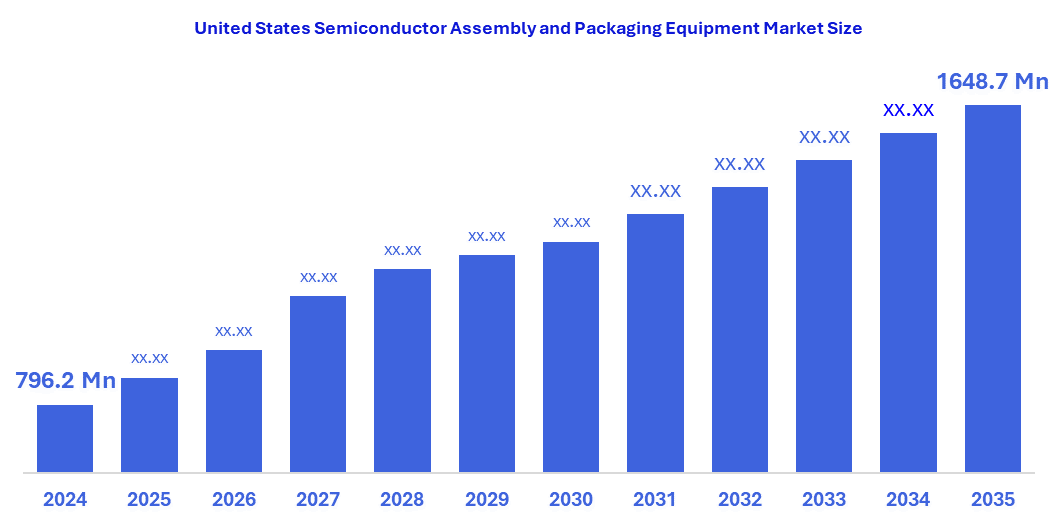
According to a research report published by Spherical Insights & Consulting, the United States Semiconductor Assembly and Packaging Equipment Market?Size is Anticipated to reach USD 1648.7 Million by 2035, Growing at a CAGR of 6.84% from 2025 to 2035. The U.S. semiconductor assembly and packaging equipment market is being driven by a rising rental demand, urban expansion, and the incorporation of digital technologies. Improved operational efficiency and a shift toward professional management solutions are accelerating market growth.
Market Overview
Semiconductor assembly and packaging equipment includes special equipment and devices used in back-end production operations of semiconductor equipment. Wafers should be chopped, assembled, packed, and tested after construction to make integrated circuits (ICS) or chips. The packaging provides electrical connections, mechanical protection, and thermal waste that semiconductor devices need to function properly in the electronic system. The assembly and packaging process consists of several stages, including wafer dish, dye bonding, wire bonding or flip-chip bonding, encapsulation, and final testing. Additionally, these activities also require dieing machines, dye bonders, wire bonders, flip-chip bonders, molding machines, packaging testers, and inspection systems. The industry has adopted refined techniques, including traditional wire bonding and wafer-level chip scale packaging (WLCSP), fan-out packaging, and 3D stacking, allowing high density and rapid signal transmission. Moreover, stability targets affect equipment design to reduce the goal of physical use, energy consumption, and semiconductor manufacturing. The semiconductor assembly and packaging equipment industry is highly innovation-driven, with continuous advancements in chip miniaturization and heterogeneous integration. Furthermore, innovation is essential to meet the growing performance and efficiency demands of sectors like automotive, aerospace, and consumer electronics. Frequent technological upgrades help firms maintain competitiveness in a rapidly evolving market.
Report Coverage
This research report categorizes the USA semiconductor assembly and packaging equipment market based on various segments and regions, and forecasts revenue growth and analyses trends in each submarket. The report analyses the key growth drivers, opportunities, and challenges influencing the USA semiconductor assembly and packaging equipment market. Recent market developments and competitive strategies, such as expansion, type launch, development, partnership, merger, and acquisition, have been included to draw the competitive landscape in the market. The report strategically identifies and profiles the key market players and analyses their core competencies in each sub-segment of the U.S. semiconductor assembly and packaging equipment market.
Driving Factor
The U.S. semiconductor assembly and packaging equipment market is driven by consumers experience with electronics, electric vehicles, 5G signs, and artificial intelligence applications. Small, high-performance semiconductor and advanced packaging technologies, such as 3D stacking and wafer-level packaging, are investing in novel equipment. Improves automation and accuracy, efficiency, and yield in production, hence promotes market expansion.
Restraining Factor
The US semiconductor assembly and packaging equipment market has to face restrictions due to High capital costs, complex technology integration, and often changing standards, all limit market expansion. The need for continuous R&D to keep the supply chain disruption, efficient labor shortage, and innovation creates challenges for US semiconductor assembly and packaging equipment manufacturers.
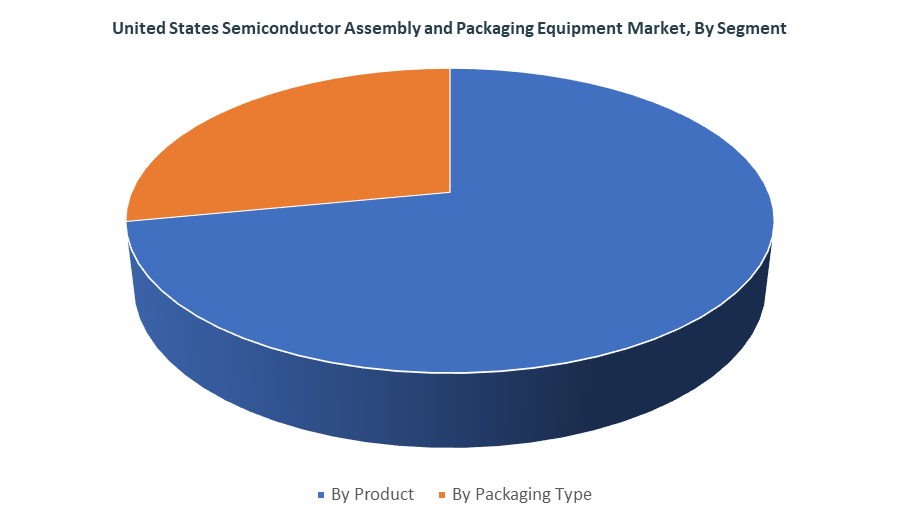
The United States semiconductor assembly and packaging equipment market share is classified into product and packaging type.
- The bonding equipment segment accounted for the largest market?share in 2024 and is anticipated to grow at a substantial CAGR during the forecast period.
The United States semiconductor assembly and packaging equipment market is segmented by product into dicing equipment, bonding equipment, packaging equipment, and others. Among these, the bonding equipment segment accounted for the largest market?share in 2024 and is anticipated to grow at a substantial CAGR during the forecast period. Bonding equipment plays an important role in attached and wire bonding processes. These techniques are important for high-color packaging in areas including motor vehicle electronics, demonstrations, and mobile devices. Manufacturers in the United States prioritize bonding technologies that allow for miniature and high-speed data transmission. Continuous push for 3D and asymmetrical integration increases the demand for sophisticated bonding solutions.
- The wafer-level packaging equipment dominated market in 2024 and is expected to grow at a significant CAGR during the projected timeframe.
The United States semiconductor assembly and packaging equipment market is segmented by packaging type into flip chip packaging equipment, wafer level packaging (WLP) equipment, fan-out packaging equipment, system-in-package (SIP) equipment, and others. Among these, the wafer-level packaging equipment dominated market in 2024 and is expected to grow at a significant CAGR during the projected timeframe. This is due to an ability to offer small, high-performance high-demonstrations with small connection length and high thermal efficiency. It is usually used in smartphones, wearables, and automotive electronics, where compactness and performance are important. wafer-level packaging is popular among semiconductor companies in the US due to its scalability and interpreting with automated manufacturing lines. Its inclusion in advanced node construction confirms its dominance.
Competitive Analysis
The report offers the appropriate analysis of the key organizations/companies involved within the United States semiconductor assembly and packaging equipment market, along with a comparative evaluation primarily based on their type of offering, business overviews, geographic presence, enterprise strategies, segment market share, and SWOT analysis. The report also provides an elaborative analysis focusing on the current news and developments of the companies, which includes type development, innovations, joint ventures, partnerships, mergers & acquisitions, strategic alliances, and others. This allows for the evaluation of the overall competition within the market.
List of Key Companies
- Applied Materials
- ASM Pacific Technology
- Besi
- Disco Corporation
- Kulicke & Soffa Industries, Inc.
- Lam Research Corporation
- Nikon Corporation
- Plasma-Therm
- Others
Key Target Audience
- Market Players
- Investors
- End-users
- Government Authorities
- Consulting and Research Firm
- Venture capitalists
- Value-Added Resellers (VARs)
Market Segment
This study forecasts revenue at the United States, regional, and country levels from 2020 to 2035. Decision Advisors has segmented the United States semiconductor assembly and packaging equipment market based on the below-mentioned segments:?
United States Semiconductor Assembly and Packaging Equipment Market, By Product
- Dicing Equipment
- Bonding Equipment
- Packaging Equipment
- Others
United States Semiconductor Assembly and Packaging Equipment Market, By Packaging Type
- Flip Chip Packaging Equipment
- Wafer Level Packaging (WLP) Equipment
- Fan-Out Packaging Equipment
- System-in-Package (SIP) Equipment
- Others
FAQ’s
Q: What is the market size of the United States Semiconductor Assembly and Packaging Equipment market in 2024?
A: The U.S. semiconductor assembly and packaging equipment market was valued at USD 796.2 million in 2024.
Q: What is the expected US Semiconductor Assembly and Packaging Equipment market size by 2035?
A: The market is projected to reach USD 1,648.7 million by 2035.
Q: What is the expected CAGR of the US Semiconductor Assembly and Packaging Equipment market during 2025–2035?
A: The market is expected to grow at a CAGR of 6.84% during the forecast period.
Q: What are the key driving factors of the US Semiconductor Assembly and Packaging Equipment market?
A: The market is driven by growing demand from consumer electronics, electric vehicles, 5G deployment, and AI applications. Advanced packaging technologies, miniaturized chips, and automation in production further fuel growth.
Q: What are the major restraining factors?
A: High capital costs, complex technology integration, rapidly changing standards, supply chain disruptions, and skilled labor shortages restrict market expansion.
Q: Which product dominated the US Semiconductor Assembly and Packaging Equipment market in 2024?
A: The bonding equipment held the largest market share in 2024 and is expected to maintain significant growth due to its importance in wire bonding and die attachment processes.
Q: Which packaging type dominated in 2024?
A: Wafer-level packaging (WLP) equipment dominated the market in 2024 and is anticipated to grow substantially, driven by compact, high-performance applications in smartphones, wearables, and automotive electronics.
Q: What are the key applications of semiconductor assembly and packaging equipment?
A: Applications include consumer electronics, automotive electronics, mobile devices, high-performance computing, and AI-driven devices requiring miniaturization and high-speed data transmission.
Q: Who are the major players in the US Semiconductor Assembly and Packaging Equipment market?
A: Key companies include Applied Materials, ASM Pacific Technology, Besi, Disco Corporation, Kulicke & Soffa Industries, Lam Research Corporation, Nikon Corporation, and Plasma-Therm.
Q: What is the forecast period covered in this report?
A: The report covers historical data from 2020–2023, with forecasts from 2025 to 2035.
Check Licence
Choose the plan that fits you best: Single User, Multi-User, or Enterprise solutions tailored for your needs.
We Have You Covered
- 24/7 Analyst Support
- Clients Across the Globe
- Tailored Insights
- Technology Tracking
- Competitive Intelligence
- Custom Research
- Syndicated Market Studies
- Market Overview
- Market Segmentation
- Growth Drivers
- Market Opportunities
- Regulatory Insights
- Innovation & Sustainability
Report Details
| Scope | Country |
| Pages | 250 |
| Delivery | PDF & Excel via Email |
| Language | English |
| Release | Sep 2025 |
| Access | Download from this page |